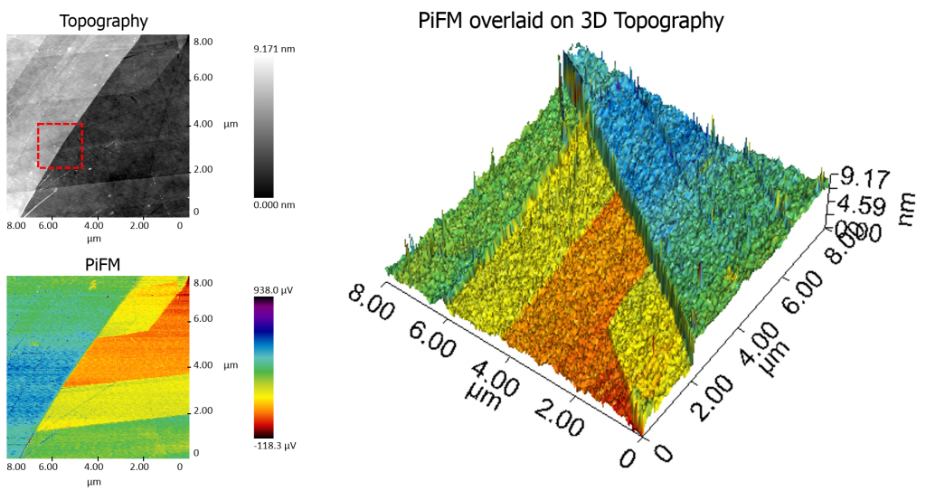
Nanoscale Identification of MoS2 Layers and Defects
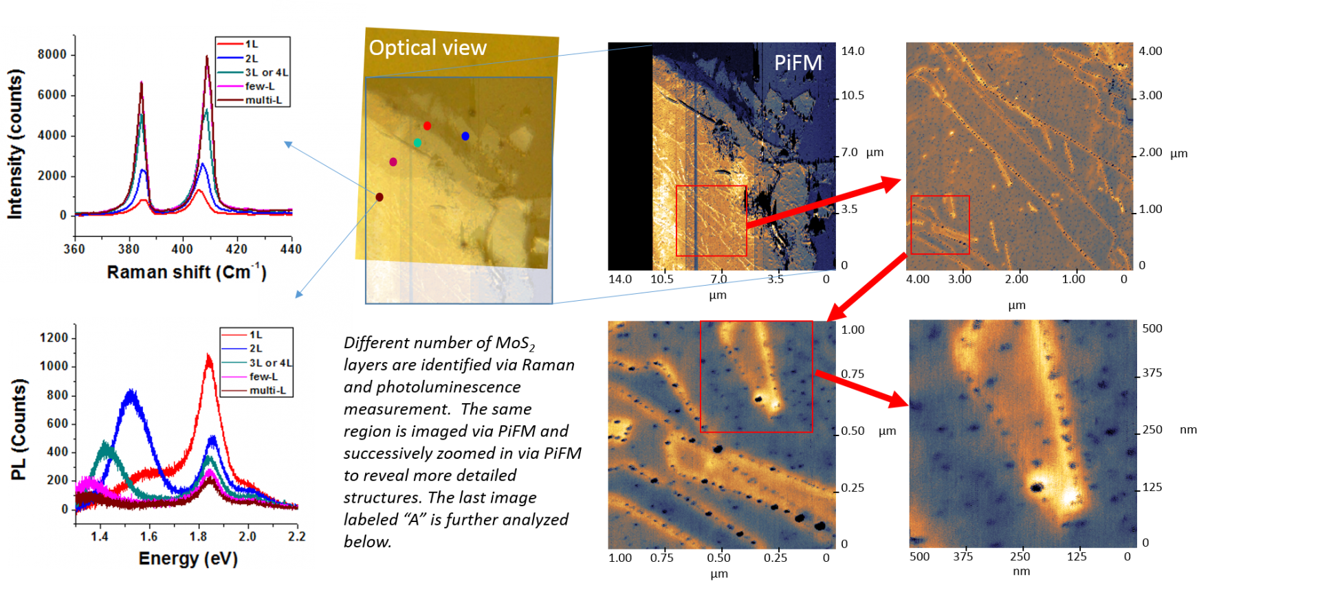
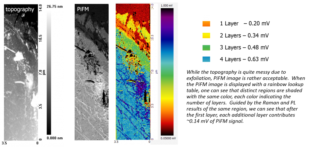
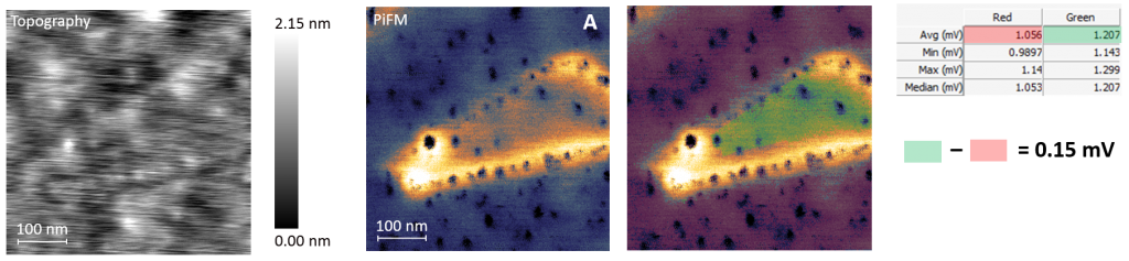
Layers in MoS2 can be identified by photoluminescence or Raman spectroscopy, both of which suffer from diffraction limit of far-field optics. Here we demonstrate that visible PiFM can detect number of layers as well as defect associated PiFM signals with exceptional sensitivity and spatial resolution. The sample below is exfoliated MoS2 film transferred onto a quartz substrate. The PiFM measurements were performed with excitation wavelength of 488 nm.
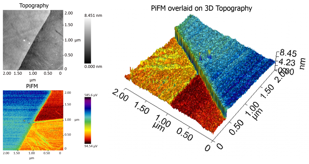
Monolayer Detection on MoSe2
Since PiFM measures the sample’s polarizability, the sample does not need to be at a resonance to produce PiFM signal. With almost all samples, PiFM generates excellent contrast between different materials due to their different optical response at a given wavelength. In this example, PiFM is able to detect the presence of monolayer of material, which is difficult to discern from topography.
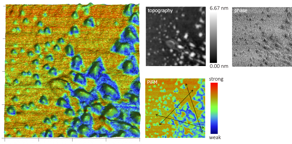
Growth of grains are seen as MoSe2 is laser heated in the presence of phosphorus. While AFM topography shows random grain structure, PiFM signal shows that triangular region surrounding each grain has very weak PiFM signal suggesting the presence of a thin layer of material with a unique optical property. The triangular layer seems to be aligned to the hexagonal lattice of the MoSe2 underlayer. (excitation wavelength = 12.2 μm, 1μm x 1 μm image)
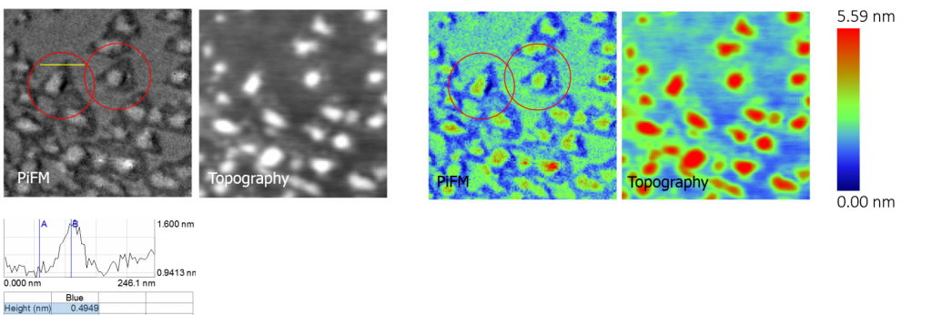
The triangular shapes in PiFM can be correlated features in topography when guided by the PiFM outline (look for the ones circled in red). By using an extreme look-up table (images on the right), the triangular shapes in topography become more recognizable. The cross-section in topography (along region corresponding to the yellow line in PiFM image) reveals that the triangular layer is about 0.5 nm thick, suggesting that the triangular regions may be monolayer of material.
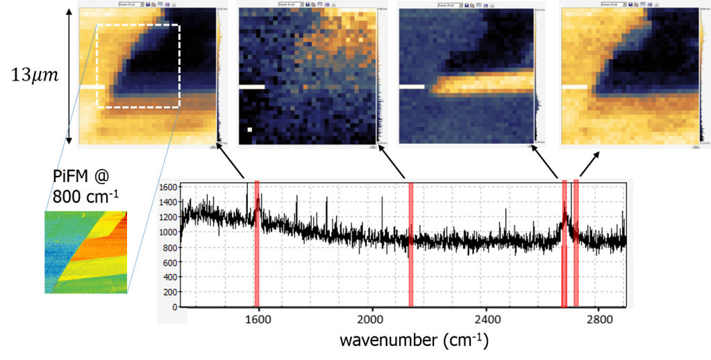
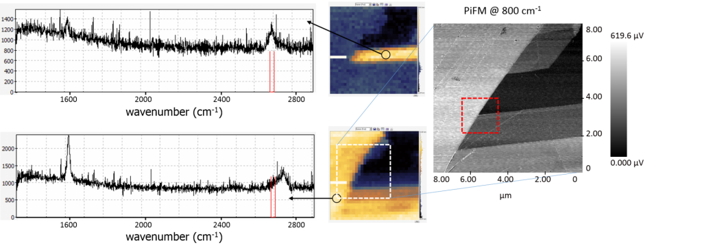
Confocal Raman Mapping and PiFM on Graphene
Copyright Molecular Vista Inc and Acutance Ltd 2021